In the modern electronics landscape, the shift from Megabytes (MB) to Gigabytes (GB) in memory storage has fundamentally changed the requirements for production-line programming. High-density devices, such as UFS (Universal Flash Storage) and eMMC (embedded MultiMediaCard), are now standard in everything from electric vehicle (EV) infotainment systems to AI-driven smart home appliances.
As the density of these integrated circuits (ICs) increases, so does the complexity of their internal architecture. Traditional programming methods that relied on simple serial communication are no longer sufficient. Modern ICs utilize multi-lane data transfers and complex handshake protocols that require precise timing and high-speed signal processing.

For engineering teams, these complexities often manifest as "hidden" bottlenecks—issues that don't just slow down production, but can lead to latent defects in the field if not addressed during the initial programming phase.
The most immediate bottleneck in high-density device programming is the raw data transfer rate. When dealing with eMMC or UFS devices used in automotive or mobile applications, the file sizes often range from several gigabytes to over 100GB. If the programming system relies on outdated interface standards, the programming time per chip can exceed several minutes, creating a massive backlog in high-volume manufacturing.
![]()
Traditional programmers often use USB 2.0 or legacy serial interfaces to communicate between the host PC and the programming site. These interfaces top out at theoretical speeds that are far below the native write capabilities of the IC.
The FPGA Solution: To overcome these bandwidth ceilings, high-performance systems utilize an FPGA-based architecture. By implementing the memory controller logic directly within the FPGA hardware, the system can achieve near-native write speeds by eliminating the latency introduced by software-based drivers and standard PC bus limitations.
Without high-speed hardware acceleration, the only way to maintain production throughput is to increase the number of programming sockets, which leads to higher capital expenditure (CAPEX) and a larger factory footprint.
As programming speeds increase to accommodate high-density UFS and eMMC devices, signal integrity (SI) becomes a critical engineering challenge. At high frequencies, the electrical signals traveling between the programmer and the IC behave like electromagnetic waves rather than simple on-off currents. Any mismatch in the transmission path can result in data corruption.
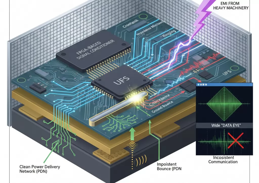
In a factory environment, Electromagnetic Interference (EMI) from nearby heavy machinery or power supplies can further degrade signal quality. Without advanced shielding and optimized trace routing, high-density programming becomes inconsistent, leading to higher "Retest" rates and lower yield.
Engineers must ensure that the programming hardware utilizes a clean power delivery network (PDN) and high-quality high-speed interconnects. Systems that integrate FPGA-based signal conditioning allow for fine-tuning of timing parameters, which helps in compensating for trace-length disparities and maintaining a wide "data eye" for stable communication.
While much focus is placed on the write speed of the IC itself, a frequently overlooked bottleneck is Image Loading Latency. In high-volume production, the time it takes to move a 32GB or 64GB firmware image from a central server or local host PC into the programmer’s internal buffer can create significant "dead time" in the manufacturing cycle.
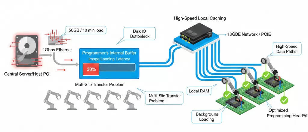
In multi-site programming systems, the challenge is compounded. If the system architecture relies on a single shared bus to load images to multiple programming heads sequentially, the overhead grows linearly with the number of sites.
Optimizing Throughput: To eliminate this delay, advanced programming systems utilize high-speed local caching and dedicated data paths for each site. By leveraging PCIe-based interconnects or 10GbE network interfaces, the image loading phase can be performed in the background or at speeds that match the internal flash write cycles, ensuring the machine remains in a state of "continuous motion."
In a high-throughput manufacturing environment, the physical interface between the programmer and the IC—the programming socket—is often the weakest link. For high-density devices like BGA (Ball Grid Array) UFS or eMMC, the socket must maintain perfect electrical contact with hundreds of microscopic solder balls simultaneously.
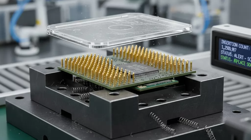
Sockets are high-precision consumables with a finite life cycle, typically rated for a specific number of "insertions." In 24/7 production lines, these limits are reached quickly, leading to several mechanical bottlenecks:
Preventative Maintenance vs. Reactive Downtime: Relying on "failure-based" maintenance is a major bottleneck. Advanced systems track insertion counts at the software level, allowing engineers to replace sockets before they cause yield drops. Utilizing high-durability sockets with gold-plated pogo pins ensures that the mechanical interface doesn't become the limiting factor for high-speed FPGA-driven programming.
Without a robust mechanical strategy, even the fastest electronic programming architecture will be throttled by frequent machine stops and manual interventions.
Beyond physical hardware limits, the software stack often introduces significant latency. In many traditional programming systems, every data packet sent to the IC must pass through multiple layers: the application software, the operating system (OS) kernel, the USB/Ethernet drivers, and finally the programmer’s firmware. This chain creates "command latency"—a delay between the instruction being sent and the chip actually executing the write command.
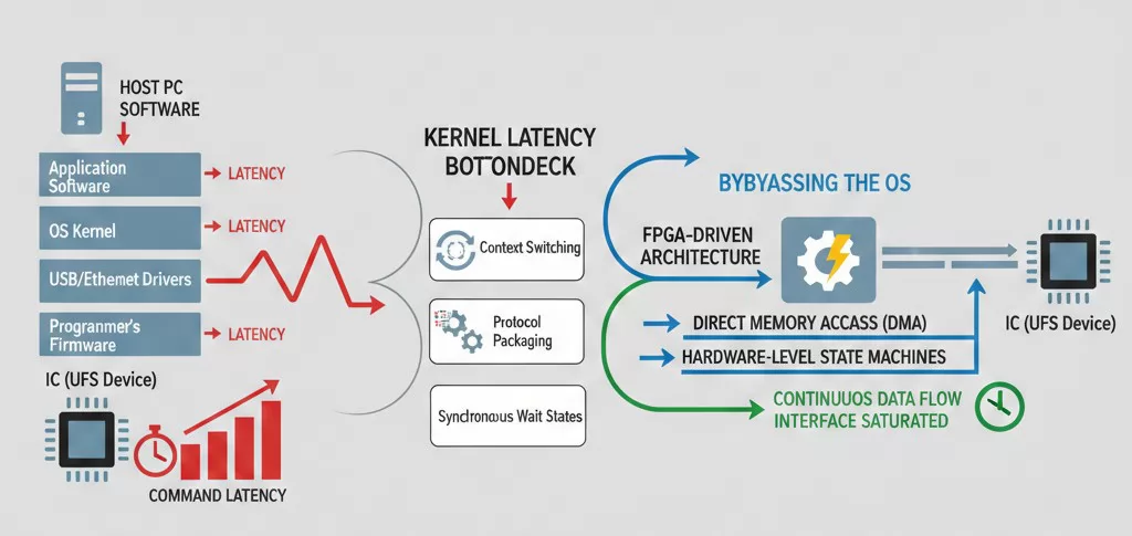
When programming high-density devices like UFS, which require complex handshaking and state-machine transitions, these micro-delays add up. For an image containing millions of data blocks, even a 1ms delay per block can extend the total programming time by several minutes.
Bypassing the OS: To eliminate these bottlenecks, Velomax utilizes an FPGA-driven architecture where the critical timing and protocol logic are moved from the PC software directly into the hardware logic. By using Direct Memory Access (DMA) and hardware-level state machines, the system can maintain a continuous data flow, ensuring that the programming interface is always saturated and never waiting on the host CPU.
For many electronics manufacturers, the bottleneck isn't the programming speed itself, but the manual handling of the ICs. While manual desktop programmers are cost-effective for small-batch prototyping, they become a major liability as production volumes scale. The transition from manual to automated programming is where many companies experience a "scalability gap."
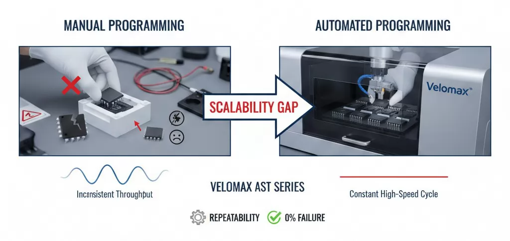
The AST Series Advantage: To bridge this gap, high-density production requires systems like the Velomax AST Series. These systems integrate high-speed AeroSpeed programmers with precision robotics, capable of handling thousands of Units Per Hour (UPH). By automating the "pick-program-place" cycle, manufacturers eliminate human-induced bottlenecks and achieve the precision required for high-density UFS and eMMC devices.
Moving to automation is not just about speed; it is about repeatability. For automotive and medical applications, where 0% failure rates are the standard, removing the human variable from the programming process is an engineering necessity.
In high-density programming, the "Write" cycle is only half the battle. The Verification phase—where the programmed data is read back and compared against the source image—is often the primary bottleneck. For a 128GB UFS device, a standard bit-by-bit verification can double the total TACT time, effectively halving the throughput of the production line.
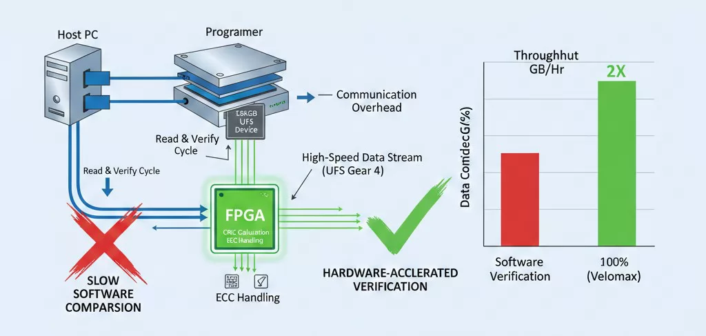
Verification is not merely a "read" operation; it is a critical quality gate. As cell sizes shrink in 3D NAND and other high-density architectures, the risk of bit flips or marginal programming increases.
FPGA-Accelerated Verification: By offloading the comparison logic to the FPGA hardware, Velomax systems can perform verification at the maximum theoretical read speed of the IC's interface (such as UFS Gear 4). This "on-the-fly" validation ensures that data integrity is guaranteed without adding significant time to the production cycle.
Without hardware-level verification, manufacturers are forced to choose between 100% data confidence and production speed—a compromise that is unacceptable in high-reliability sectors like automotive electronics.
High-density programming is a power-intensive process. When writing to multiple eMMC or UFS chips simultaneously at high frequencies, the localized heat generated by the ICs and the programming circuitry can create a significant thermal bottleneck. If not managed, this heat leads to thermal throttling—where the chip reduces its own performance to prevent damage—or worse, permanent data corruption.
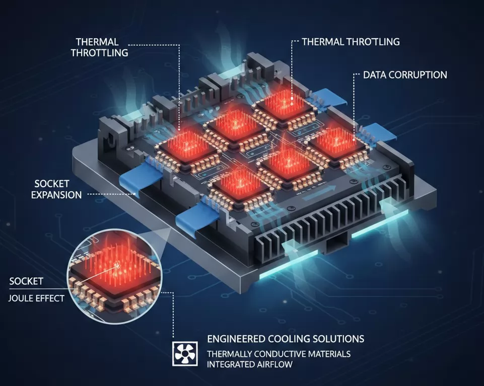
Engineered Cooling Solutions: High-performance automated systems must incorporate active thermal management. This includes utilizing thermally conductive socket materials and integrated airflow systems within the automated handler. By maintaining a stable operating temperature, the system ensures that the silicon operates within its optimal performance envelope, preventing the slowdowns associated with thermal protection circuits.
In the era of Industry 4.0, a programming system that operates as an "island" is a bottleneck to the entire manufacturing process. High-density devices often contain unique identifiers, security keys, or MAC addresses that must be logged and tracked. Without seamless MES (Manufacturing Execution System) integration, data management becomes a manual, error-prone task.
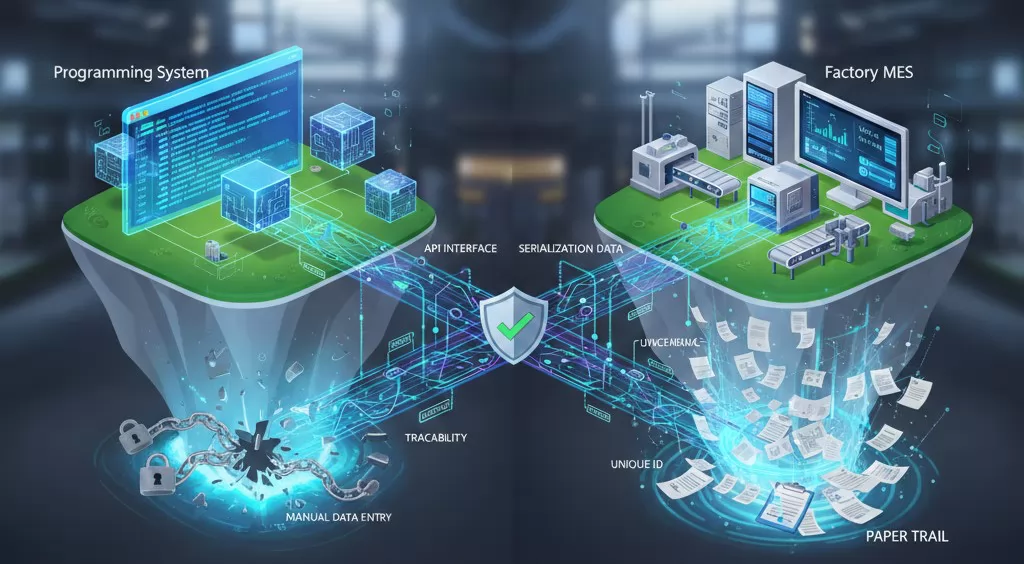
When programming high-density storage for EV or smart devices, traceability is non-negotiable. Bottlenecks typically occur in three areas:
Smart Connectivity: Modern systems utilize API-driven interfaces to communicate directly with the factory floor's software layer. This ensures that every high-density device is programmed with the correct firmware version and its unique ID is recorded without adding a single second to the cycle time. By automating the data flow, manufacturers eliminate the "paper trail" bottleneck and move toward a fully transparent production line.
The rapid evolution of high-density storage technologies—from eMMC 5.1 to UFS 4.0 and beyond—demands a programming architecture that can adapt without requiring a complete hardware overhaul. Traditional, fixed-processor programmers are inherently limited by their internal clock speeds and hardwired peripheral sets. To overcome this final bottleneck, the industry has shifted toward FPGA-based architectures.
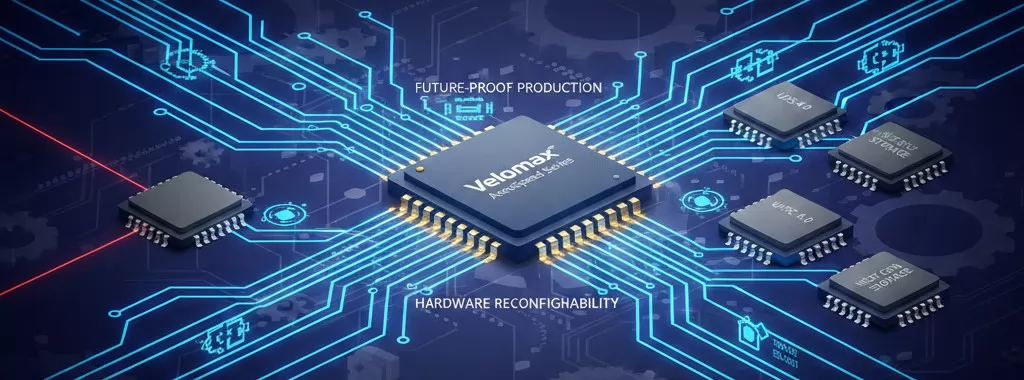
Field Programmable Gate Arrays (FPGAs) allow the programming system to "morph" its hardware logic to match the specific requirements of the IC being programmed. This provides several technical advantages:
AeroSpeed Series: The Next Generation: At Velomax, our AeroSpeed Series leverages advanced FPGA architecture to eliminate the traditional trade-off between speed and reliability. By moving the heavy lifting from software to hardware, we ensure that as IC densities continue to double, your production throughput remains uncompromised.
Discover this amazing content and share it with your network!
Your Name*
Your Email*


*We respect your confidentiality and all information are protected.