Before analyzing performance metrics and architectural nuances, it is essential to establish the fundamental definitions of these two dominant non-volatile memory standards managed by JEDEC. While both serve as embedded storage solutions for mobile and industrial devices, their underlying protocols represent different generations of storage technology.
eMMC consists of NAND flash memory and a simple controller packaged into a single integrated circuit. It is the traditional standard for mobile storage, evolved from the MMC format. Its architecture is based on a parallel interface, which simplifies circuit design but inherently limits maximum data transfer speeds. eMMC is widely regarded as a cost-effective solution for legacy systems, budget smartphones, and static industrial applications where ultra-high speed is not critical.
UFS represents the shift towards high-performance embedded storage, designed to bring SSD-class speeds to mobile and embedded systems. Unlike eMMC, UFS utilizes a serial interface with a full-duplex LVDS (Low-Voltage Differential Signaling) serial link. This architecture supports Command Queueing (CQ), allowing the system to handle multiple read/write commands simultaneously. UFS is increasingly becoming the standard for automotive ADAS, high-end mobile devices, and complex edge computing systems.
Key Distinction: The transition from eMMC to UFS is comparable to the shift from PATA (IDE) drives to SATA SSDs in the PC industry. While eMMC relies on a simpler 8-bit parallel bus, UFS leverages MIPI M-PHY physical layers to achieve significantly higher bandwidth.
The primary divergence between eMMC and UFS lies in how data is physically transmitted between the host processor and the storage device. This architectural shift dictates not only the maximum potential bandwidth but also the efficiency of the data flow.
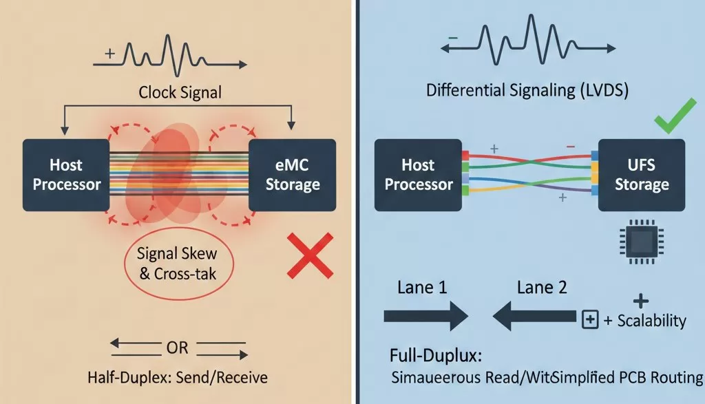
eMMC utilizes an 8-bit parallel interface. In this legacy architecture, data bits are sent across multiple wires simultaneously, synchronized by a single clock signal.
UFS abandons the parallel bus in favor of a high-speed serial interface, leveraging the MIPI M-PHY (Physical Layer) standard. This design is similar to the architecture found in PCIe or SATA interfaces used in desktop computing.
Engineering Note: While the UFS controller is more complex than that of eMMC, the reduction in pin count for data transmission (despite the differential pairs) often simplifies PCB routing for high-frequency signal integrity.
The architectural differences explored in Chapter 2 translate directly into vastly different real-world performance metrics. Throughput is arguably the most critical factor influencing device boot-up times, application loading, and overall user experience in high-demand systems.
Sequential speed measures the maximum rate at which large, continuous blocks of data can be transferred (e.g., loading a large operating system file or recording a 4K video stream). This is where UFS demonstrates its most significant advantage.
| Standard Version | eMMC Max Throughput (MB/s) | UFS Max Throughput (MB/s) |
|---|---|---|
| Entry/Mid-Level | eMMC 5.1: up to 400 | UFS 2.1: up to 1,200 |
| High-Performance | N/A | UFS 3.1: up to 2,900 |
| Next-Gen | N/A | UFS 4.0: up to 4,600 |
The practical limit for eMMC 5.1 is capped at roughly 400 MB/s due to the overhead of the parallel bus and its half-duplex nature. In contrast, UFS versions achieve nearly an order of magnitude higher performance by leveraging faster MIPI M-PHY Gears and the ability to operate in full-duplex mode.
Random speed is a better indicator of system responsiveness, measuring how quickly the device can access scattered, small blocks of data—critical for multitasking and database operations. UFS excels here due to Command Queueing (CQ).
Manufacturing Consideration: Higher throughput directly impacts the programming time on the production line. For high-density, high-volume products, UFS programmers must be capable of sustaining these multi-gigabit speeds flawlessly to minimize cycle time.
The duplexing mode defines whether data can be transmitted in one direction or both directions simultaneously. This is a crucial design limitation impacting the efficiency of complex tasks that require simultaneous reading (from memory) and writing (to memory or other peripherals).
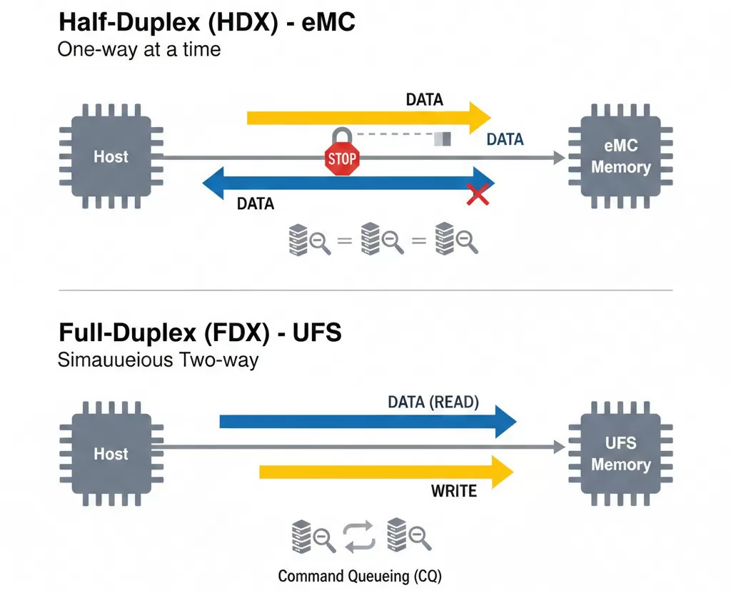
The eMMC interface operates in Half-Duplex mode. This means that the physical bus wires can only be used for one operation at a time: either the host reads data from the memory, or the host writes data to the memory. It cannot do both concurrently.
UFS leverages its MIPI M-PHY architecture to enable Full-Duplex operation. The UFS bus consists of dedicated transmit lanes and dedicated receive lanes. This enables concurrent two-way data flow:
Engineering Rationale: Full-Duplex capability is essential for devices requiring high-concurrency operations, such as high-resolution automotive cameras (simultaneous recording and processing) or high-density server-grade storage devices.
While sequential speed defines raw data transfer capacity, IOPS (Input/Output Operations Per Second) and Latency are the metrics that truly define the feel and responsiveness of a computing device. High IOPS and low latency are critical for ensuring quick application launches and seamless multitasking.
IOPS measures the number of read or write requests that a storage device can handle in one second. This metric is predominantly driven by random access performance.
Latency is the delay between when the host issues a command and when the data transfer actually begins. Latency is the primary cause of perceived lag in a device.
The UFS protocol is specifically designed to minimize latency, particularly in the random access domain. The ability to manage a queue of commands means that the storage device rarely sits idle waiting for the host to issue the next instruction. Furthermore, the efficient serial link (M-PHY) has lower clock-to-data-ready overhead compared to the complex synchronization required by the parallel eMMC bus.
| Metric | eMMC Characteristic | UFS Characteristic |
|---|---|---|
| IOPS | Low (Single-digit K) | High (Tens to Hundreds of K) |
| Latency | Higher, particularly under load | Significantly Lower and Consistent |
Technical Impact: For applications requiring consistent, real-time data logging and processing—such as electric vehicle (EV) telemetry or automated factory control—the low and predictable latency of UFS is mandatory. High-speed programming systems must validate these latency figures during production testing.
For mobile, automotive, and battery-powered embedded devices, storage power consumption is a critical design parameter. While UFS offers superior performance, its power management features are also significantly more advanced than those of eMMC.
Due to its high clock speeds and complex controller, a UFS device typically consumes more peak power than an eMMC module during high-demand operation (e.g., maximum sequential reads). However, the superior speed of UFS means that it can complete required tasks much faster. This leads to what engineers call the "race-to-sleep" advantage.
UFS standards incorporate sophisticated power states, leveraging the MIPI M-PHY layer, which are not available in eMMC:
Thermal Design: Higher data throughput in UFS leads to brief, intense bursts of heat generation, requiring careful thermal management, particularly in high-density applications like EV infotainment systems. eMMC generates heat more slowly but consistently over a longer operational period.
The choice between eMMC and UFS is ultimately dictated by the application's specific requirements for speed, power, cost, and endurance. Selecting the wrong standard can lead to performance bottlenecks or unnecessary cost overhead.
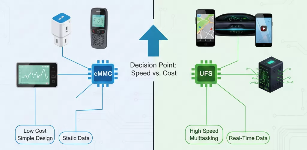
eMMC remains a highly relevant standard for applications that prioritize low cost, simplified design, and relatively static data storage. Its mature technology and reliable performance at lower speeds make it suitable for:
UFS is the mandatory choice for modern, data-intensive, and concurrent processing environments. The full-duplex speed and Command Queueing are essential for these sectors:
Decision Point: If the device relies on streaming or real-time data processing (like high-speed logging or simultaneous read/write), UFS is required. If the storage is primarily for static OS loading and cost is the main driver, eMMC may suffice.
For manufacturers of high-end devices utilizing UFS and high-density eMMC, the production phase—specifically the programming and testing of the embedded memory—introduces significant technical and logistical challenges.
As memory densities increase (e.g., from 64 GB to 1 TB and beyond) and UFS throughput jumps (UFS 3.1 and 4.0), the time required to program the necessary firmware and application data becomes a critical bottleneck in the manufacturing cycle time. Programming 1 TB of data onto a UFS 4.0 module at its theoretical peak requires high-performance, sustained data transfer across all programming sockets simultaneously.
The transition from eMMC's slower parallel bus to UFS's high-speed serial MIPI M-PHY interface drastically increases the complexity of maintaining signal integrity during the programming process. Any noise, impedance mismatch, or poor contact quality can lead to programming failure or data corruption.
Velomax Expertise: Programming systems must transition from simply pushing data to acting as high-speed data validation engines. This requires dedicated hardware, like the FPGA-powered systems (e.g., Velomax's AeroSpeed Series), which are engineered for ultra-fast, flawless execution of UFS and high-density eMMC programming.
The trajectory of embedded storage technology clearly points toward the increasing dominance of UFS across virtually all market segments, driven by rising data requirements and the demand for instant responsiveness.

While eMMC once held a significant cost advantage, the price differential between high-end eMMC and entry-level UFS (UFS 2.x) continues to narrow. As manufacturing efficiencies for UFS controllers improve, the performance trade-off for choosing eMMC becomes harder to justify, even for mid-range devices.
JEDEC continues to expand the UFS ecosystem to cover more use cases:
The high-performance requirements of Artificial Intelligence (AI) and Machine Learning (ML) inference models running at the edge necessitate faster memory access. These computationally intense tasks rely on consistent, low-latency I/O to quickly load model weights and process real-time data streams, making the speed and IOPS capabilities of UFS mandatory for next-generation devices.
Manufacturing Preparedness: Manufacturers must invest in programming infrastructure (like high-speed, FPGA-based programmers) that can support the current and future standards of UFS (e.g., UFS 4.0), ensuring their production capabilities do not become obsolete before the product lifecycle ends.
The decision between eMMC and UFS must be holistic, balancing the performance requirements of the application with cost, power, and manufacturing readiness. There is no single "best" standard, only the most appropriate one for the specific device ecosystem.
| Feature | eMMC Standard (e.g., 5.1) | UFS Standard (e.g., 3.1) |
|---|---|---|
| Interface | Parallel (8-bit) | Serial (MIPI M-PHY) |
| Duplexing | Half-Duplex (Read or Write) | Full-Duplex (Read and Write) |
| Max Speed (Approx.) | ~400 MB/s | ~2,900 MB/s (UFS 3.1) / ~4,600 MB/s (UFS 4.0) |
| I/O Command | Single Command | Command Queueing (CQ) |
| Latency | High/Variable | Low/Consistent |
| Best for | Cost-sensitive, low-concurrency IoT, Basic HMIs | High-performance mobile, Automotive ADAS, Edge AI |
For engineers designing next-generation products, the following criteria should guide the final choice:
The industrial trend is clear: UFS is the future. While eMMC retains a niche in highly cost-sensitive sectors, any device requiring high-speed programming, concurrency, or robust performance should adopt UFS.
Discover this amazing content and share it with your network!
Your Name*
Your Email*


*We respect your confidentiality and all information are protected.