
For B2B buyers—such as OSAT facilities, EMS contract manufacturers, procurement managers, and automotive electronics manufacturing leads—selecting the right equipment supplier is critical to ensuring production yields, minimizing line downtime, and scaling throughput.
Whether you are expanding a wafer fab, setting up an advanced packaging facility, or optimizing high-speed backend IC device programming and testing lines, having a clear list of established vendors streamlines vendor evaluation.
Below is a detailed guide to the Top 10 Semiconductor Equipment Manufacturers in the USA for 2026, ranked by market leadership, technological breadth, and industry footprint, followed by specialized recommendations for high-efficiency backend IC device handling and programming solutions.
10. Cohu, Inc.

Headquarters: Santa Clara, California
Primary Products: Chemical Vapor Deposition (CVD), Physical Vapor Deposition (PVD), Atomic Layer Deposition (ALD), Chemical Mechanical Planarization (CMP), Etch, Metrology, and Inspection equipment.
Target Market Focus: Advanced logic foundries, DRAM and NAND memory manufacturers, and advanced packaging facilities requiring integrated materials engineering solutions.
Global Supply Chain Footprint: Extensive global logistics networks with primary R&D and manufacturing facilities in the United States, Singapore, Taiwan, Korea, and Europe.
Overview:
As one of the world's premier semiconductor equipment manufacturers, Applied Materials provides broad capabilities across materials engineering, supplying equipment used to produce virtually every new chip and advanced display in the world. The company specializes in front-end wafer processing systems, offering solutions that enable atomic-scale chip fabrication and complex 3D integration architectures.
Headquarters: Fremont, California
Primary Products: Plasma Etch systems, Selective Etching tools, Single-wafer and Batch Clean systems, Chemical Vapor Deposition (CVD), and Electroplating systems.
Target Market Focus: High-volume memory fabricators (3D NAND, High Bandwidth Memory/HBM), leading-edge logic foundries, and specialty technology markets.
Global Supply Chain Footprint: Major manufacturing and technical centers located across North America, Asia (including Korea, Taiwan, and Malaysia), and Europe.
Overview:
Lam Research is a leading global supplier of wafer fabrication equipment and services to the semiconductor industry. Recognized among top semiconductor equipment manufacturers, Lam’s product portfolio focuses on etch, deposition, and clean technologies that allow chipmakers to build smaller, faster, and more power-efficient devices essential for artificial intelligence and high-performance computing.

Headquarters: Milpitas, California
Primary Products: Wafer Inspection Systems, Reticle Inspection, Optical and Electron-beam Metrology Systems, Process Control Software, and Advanced Packaging Inspection Tools.
Target Market Focus: Semiconductor wafer fabs, mask shops, and OSAT packaging providers looking to maximize process yield and inline quality control.
Global Supply Chain Footprint: Operations, engineering centers, and regional support infrastructure distributed across the United States, Europe, Israel, and the Asia-Pacific region.
Overview:
KLA Corporation is an industry leader in process control and yield management. As one of the most essential semiconductor equipment manufacturers, KLA develops advanced inspection and metrology tools, along with data analytics platforms, to help chip manufacturers detect nanometer-scale defects and ensure operational efficiency throughout the manufacturing flow.
Headquarters: North Reading, Massachusetts
Primary Products: Automated Test Equipment (ATE), System-on-Chip (SoC) test platforms, Memory Test Systems, System Level Testing (SLT) equipment, and Industrial Automation tools.
Target Market Focus: OSAT facilities, IDMs, fabless chip designers, automotive electronics original manufacturers, and high-reliability industrial production lines.
Global Supply Chain Footprint: Comprehensive worldwide technical support, applications engineering centers, and supply partners across North America, Europe, and Asia.
Overview:
Teradyne brings high-accuracy automated testing solutions to market, ensuring that complex microprocessors, wireless chips, and memory modules meet strict quality criteria before final assembly. Positioned prominently among backend semiconductor equipment manufacturers, Teradyne’s testing platforms are widely utilized to accelerate time-to-market for consumer, automotive, and data center electronics.

Headquarters: Wilmington, Massachusetts
Primary Products: Automated Macro/Micro Defect Inspection Systems, Ellipsometry and Reflectometry Metrology, Lithography Systems, and Process Integration Software.
Target Market Focus: Advanced packaging (CoWoS, Chiplets), specialty semiconductor fabs (Power, RF, MEMS), and logic/memory substrate processing.
Global Supply Chain Footprint: Global service, applications development, and assembly operations supporting major semiconductor hubs in North America, Europe, and Asia.
Overview:
Formed by the merger of Rudolph Technologies and Nanometrics, Onto Innovation serves the un-fragmented semiconductor value chain from front-end wafer processing to advanced packaging. As specialized semiconductor equipment manufacturers, Onto Innovation delivers process control tools essential for high-density interconnects, power devices, and heterogeneous chiplet integration.
Headquarters: Beverly, Massachusetts
Primary Products: High-current, High-energy, and Medium-current Ion Implantation Systems (Purion platform).
Target Market Focus: Automotive power electronics (Silicon Carbide / SiC and Gallium Nitride / GaN), image sensors, mature-node logic, and specialty semiconductor fabs.
Global Supply Chain Footprint: Manufacturing headquarters in Massachusetts complemented by customer support centers across North America, Europe, and Asia.
Overview:
Axcelis Technologies designs, manufactures, and services ion implantation platforms used in the fabrication of semiconductor chips. Established as one of the premier niche semiconductor equipment manufacturers, Axcelis’s Purion technology plays a pivotal role in enabling power management chips for electric vehicles (EVs), renewable energy systems, and high-efficiency power infrastructure.
Headquarters: Plainview, New York
Primary Products: Laser Annealing Systems, MOCVD (Metalorganic Chemical Vapor Deposition) Systems, Ion Beam Etch & Deposition, and Advanced Packaging Lithography Tools.
Target Market Focus: MicroLED, compound semiconductors (GaN/GaAs), data center photonics, advanced packaging, and hard disk drive recording head manufacturing.
Global Supply Chain Footprint: R&D, manufacturing, and customer service centers operating across the United States, Europe, China, Taiwan, and Korea.
Overview:
Veeco Instruments provides process equipment technologies that drive energy-efficient applications and high-density semiconductor manufacturing. Recognized among innovative semiconductor equipment manufacturers, Veeco specializes in ion beam technologies, precision laser annealing, and MOCVD platforms required for next-generation optoelectronics and power electronics.
Headquarters: St. Petersburg, Florida
Primary Products: Inductively Coupled Plasma (ICP) Etch, Reactive Ion Etch (RIE), Plasma-Enhanced Chemical Vapor Deposition (PECVD), and High-Density Plasma CVD (HDPCVD).
Target Market Focus: Wireless/RF components, power electronics, MEMS sensors, photonics, and semiconductor failure analysis laboratories.
Global Supply Chain Footprint: US-based manufacturing with direct sales, service, and spare parts distribution hubs across the Americas, Europe, and Asia.
Overview:
Plasma-Therm is a manufacturer of plasma-process equipment catering to specialty semiconductor markets and high-mix production environments. As reliable semiconductor equipment manufacturers, Plasma-Therm supplies versatile, modular dry etching and thin-film deposition solutions optimized for power devices, compound semiconductors, and advanced packaging.

Headquarters: Livermore, California
Primary Products: Advanced Wafer Probe Cards, Analytical Probe Stations, Cryogenic Test Systems, and Thermal Subsystems.
Target Market Focus: Wafer-level testing, SoC and memory device characterization, quantum computing hardware, and silicon photonics validation.
Global Supply Chain Footprint: Worldwide network of probe card repair centers, design offices, and manufacturing plants located in North America, Europe, and Asia.
Overview:
FormFactor is a leading provider of essential test and measurement technologies across the IC lifecycle. Operating as vital backend semiconductor equipment manufacturers, FormFactor offers high-precision probe cards that allow chipmakers to test semiconductor wafers at high speeds and under extreme thermal conditions prior to packaging.
Headquarters: Poway, California
Primary Products: Pick-and-Place Test Handlers, Gravity and Turret Handlers, Thermal Subsystems, Inspection & Metrology Modules, and Test Contactors.
Target Market Focus: Automotive semiconductor test automation, OSAT backend processing, mobility, industrial electronics, and consumer device manufacturing.
Global Supply Chain Footprint: Global manufacturing, engineering, and field-service teams across North America, Europe, Asia, and major OSAT regions.
Overview:
Cohu provides test handling, thermal management, inspection, and contactor solutions for the semiconductor manufacturing industry. Listed among trusted semiconductor equipment manufacturers, Cohu’s products automate device handling during the post-fabrication test phase, ensuring high throughput, physical protection, and precise temperature control for automotive-grade and industrial microchips.
While the top 10 companies listed above dominate front-end wafer fabrication and core chip testing, modern electronics manufacturing—particularly in fast-growing sectors like electric vehicles, AIoT, and consumer hardware—demands equal efficiency during the final post-fabrication phase. For B2B buyers looking to optimize high-density IC device handling, lower cycle times, and prevent line bottlenecks, specialized backend automated solutions are essential.
If your facility requires fast, reliable, and scalable post-fab offline/inline IC programming equipment, VeloMax provides industry-leading hardware and service solutions tailored to high-density semiconductor devices.
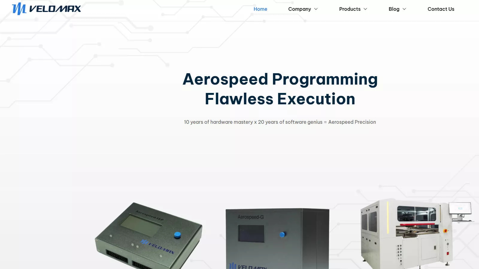
Headquarters: Singapore (Global Operations)
Primary Products: Automated IC Programming Systems (AST Series), High-Speed Manual Programmers (Aerospeed Series), Automated Handlers, and Turnkey Programming Services.
Target Market Focus: Automotive electronics manufacturers (EVs), EMS contract manufacturers, OSAT facilities, smart home appliance makers, and industrial OEM hardware developers.
Global Supply Chain Footprint: Global service, technical support, and logistics network with operational hubs and engineering teams strategically located across Asia and North America.
Overview:
VeloMax Systems is a specialized manufacturer of high-speed device programming platforms and automated IC handling equipment for post-fabrication semiconductor processing. Recognized among innovative semiconductor equipment manufacturers, VeloMax combines high-precision hardware automation with advanced FPGA software architecture. The company delivers ultra-high throughput systems (up to 3000 UPH) equipped with 2D/3D inspection, MES connectivity, and specialized UFS/eMMC programming solutions tailored for mission-critical automotive and industrial applications.
Ultra-High Throughput & Advanced Automation (UPH Leadership)
VeloMax designs advanced systems like the Automated Handler (AST-9000 & AST-1000 Series), capable of achieving production throughputs up to 3000 UPH (Units Per Hour). Featuring dual-drive linear motor technology, integrated 2D/3D vision inspection, automated tape/tray/tube repacking, and MES network connectivity, VeloMax handles complex IC packaging sizes with high precision (±0.02 mm placement accuracy).
Specialized High-Speed UFS Programming for EVs
Modern electric vehicles and smart cockpits rely heavily on high-capacity UFS and eMMC storage chips. VeloMax provides purpose-built UFS Programming Solutions for Electric Vehicles, delivering write speeds up to 3000 MB/s. This significantly reduces programming cycle times for large automotive firmware files, maintaining high yield rates and meeting stringent automotive electronics standards.
Flexible Engineering Tools for Small-Batch & Prototyping
For lab development, initial sample runs, or low-volume/high-mix assembly lines, the VeloMax Manual Programmer (such as the Aerospeed-GS series) offers high-speed FPGA-driven architecture in a compact desktop footprint, supporting broad device types including MCU, NAND/NOR Flash, eMMC, and UFS.
Turnkey Outsourced IC Programming Service
For manufacturers seeking a low-CAPEX model or immediate capacity expansion, VeloMax offers a comprehensive Programming Service. This outsourced service covers tape-and-reel repacking, 3D pin inspection, laser marking, and customized firmware loading under strict ISO-compliant quality protocols.
Navigating the US semiconductor equipment market in 2026 requires balancing high-CAPEX front-end fabrication investments with ultra-efficient, agile back-end testing and programming operations. While industry giants like Applied Materials, Lam Research, and KLA lead the way in wafer-level processing, operational success on the factory floor often hinges on eliminating bottlenecks during final IC handling and device programming.
For OSATs, EMS contract manufacturers, and automotive electronics producers looking to maximize throughput without compromising device integrity, partnering with specialized equipment suppliers is essential. By deploying high-UPH automation, vehicle-grade programming architectures, and flexible service models—such as those offered by VeloMax—procurement teams can effectively secure their production lines, improve yield rates, and maintain a competitive edge in today's rapidly evolving semiconductor landscape.
To evaluate VeloMax IC programming systems or request a custom technical assessment for your production line, visit the official VeloMax .
Discover this amazing content and share it with your network!
Your Name*
Your Email*


*We respect your confidentiality and all information are protected.
